

bricol67
-
Posts
24 -
Joined
-
Last visited
bricol67's Achievements
Member (2/9)
0
Reputation
-
Jamo D600/RT - 12D Amplifier Power Supply Circuit Repair
bricol67 replied to bricol67's topic in Technical/Restorations
I don't understand that you can't find faulty components! I summarize: -If you bypass the transistor between emitter and collector, the power supply goes into shutdown (voltage on J2 = 0) -If you force the power off mode on J3 the transistor Q4 does not react. That's right? How do you go about testing transistor Q4? -
Jamo D600/RT - 12D Amplifier Power Supply Circuit Repair
bricol67 replied to bricol67's topic in Technical/Restorations
Ok, so if you bypass Q4, the power goes to standby. So, either there is one of the broken resistors R1 / R2 / R8 / R9 or the transistor Q4. -
This is why I am asking you to shunt Q4, to confirm that it is Q4. It could still be other components. OK, see you tomorrow, have a good evening.
-
Jamo D600/RT - 12D Amplifier Power Supply Circuit Repair
bricol67 replied to bricol67's topic in Technical/Restorations
OK perfect. So your transistor Q4 or one of the resistors R1 / R2 is broken. You can try to bypass Q4 (pin 2 + 3 on the diagram) and the power supply should go on standby. -
Jamo D600/RT - 12D Amplifier Power Supply Circuit Repair
bricol67 replied to bricol67's topic in Technical/Restorations
OK. It would be necessary to measure the voltage indicated by the 2 arrows in red for the 2 modes (power on and standby).
-
Jamo D600/RT - 12D Amplifier Power Supply Circuit Repair
bricol67 replied to bricol67's topic in Technical/Restorations
16V ok -0.5v nothing no reaction: 0v! Sorry I do not understand! The voltage changes or it does not change on pin 1, if you toggle the "Power ON / standby" switch -
Jamo D600/RT - 12D Amplifier Power Supply Circuit Repair
bricol67 replied to bricol67's topic in Technical/Restorations
Ok, so the standby function doesn't work. Validate that on pin 1 the voltage does indeed change from -05 to 16v if you switch the standby mode. If this is the case, you must check the transistor Q4 and Q2 + R1 and R2. The standby principle consists of cutting off the VCC power supply from the IR2153 circuit. Not easy to take measurements with the control board in place! -
Jamo D600/RT - 12D Amplifier Power Supply Circuit Repair
bricol67 replied to bricol67's topic in Technical/Restorations
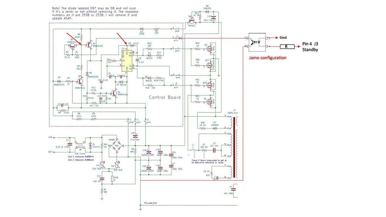
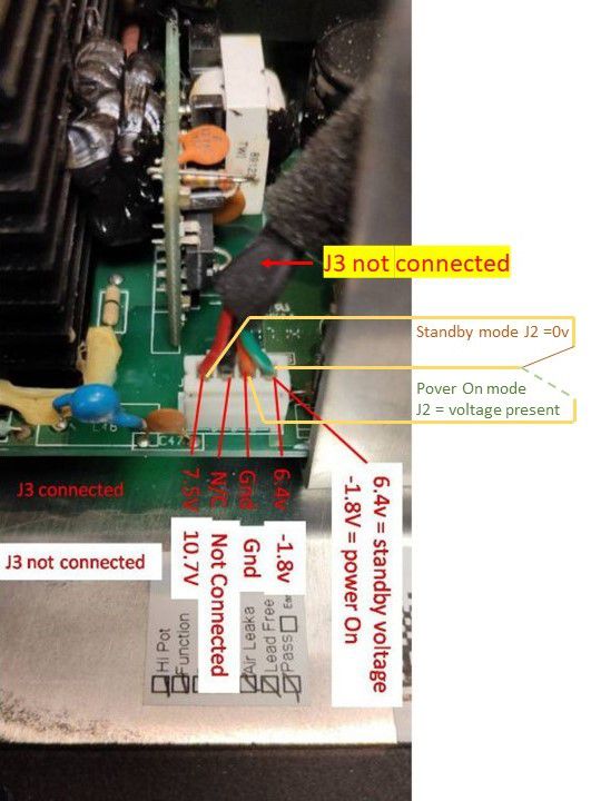
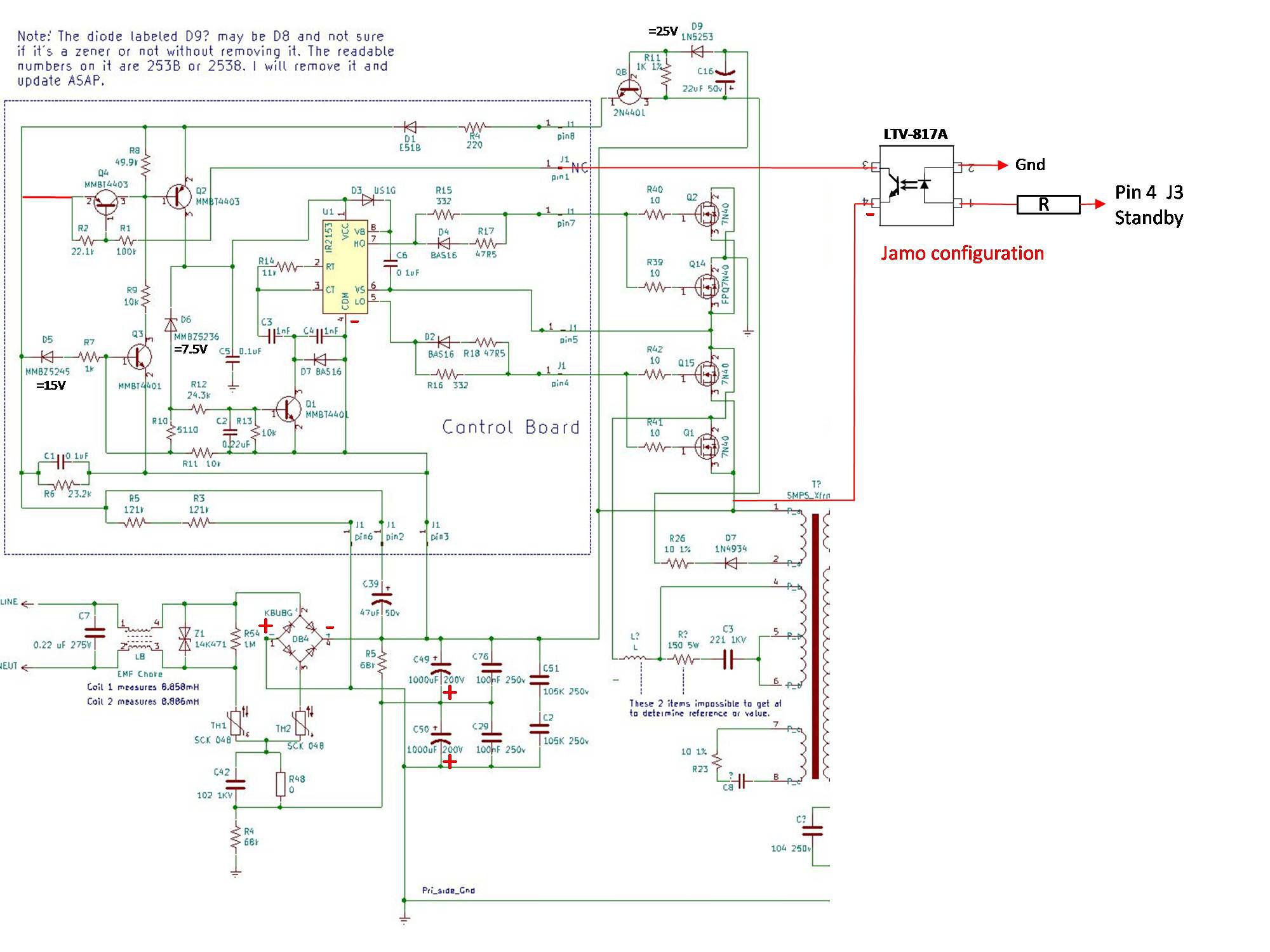
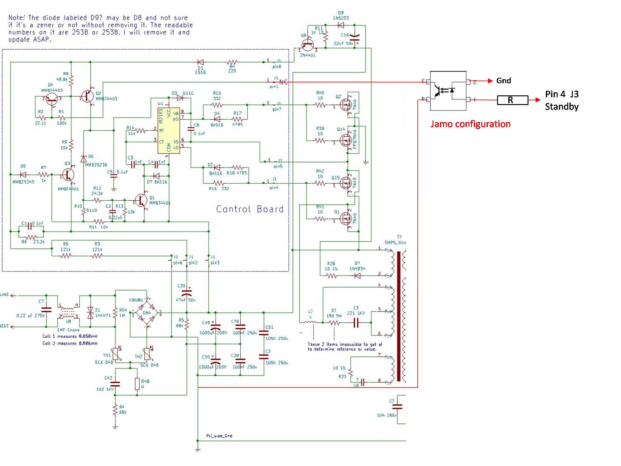
in fact the standby pin on J3 and 1 ?? On your modified diet diagram posted on 10.11 at 07:44 PM, you noted: pin 4 J3 stanby ??? Well no, it's not pin 1 it's pin 4, as shown in the photo and the diagram. Review what you scored on Saturday at 06:52 PM. It is indeed the green pine which changes voltage -2.3v => 7.1v j3 not connected (switch position on): -2.3v (orange and green) and 10.7v (red and orange) j3 connected (switch position on): 7,1v (orange and green) and 8,7v (red and orange) If you want to test the power supply alone, just put a changeover switch as in the attached photo (J2 and J3 not connected to the other boards). The voltages at the outputs on J2 must react as indicated in the post of Saturday at 02:11 PM
-
Jamo D600/RT - 12D Amplifier Power Supply Circuit Repair
bricol67 replied to bricol67's topic in Technical/Restorations
Hello Yroger, We might have misunderstood each other, but there are a couple of posts back you said: So I think it's moving forward. So we have a problem see diagram. the voltages are identical whether the J3 cable is connected or not ! If this is indeed the case, that the voltages on J2 do not go to 0, with a voltage of 8V on the standby pin of J3, your power supply is not working correctly. Can you confirm that it is working fine, if so the power supply is working. -
Jamo D600/RT - 12D Amplifier Power Supply Circuit Repair
bricol67 replied to bricol67's topic in Technical/Restorations
Good evening Roger, I just looked at the photos I took and the klipsch diagram. I hadn't paid attention, in fact there is no 110 / 220V selection on the diagram that's why there is the R48. Indeed there is an error in the direction of the diode bridge and the capacitors on the diagram and I now understand why you are measuring -313V. In fact, you have to measure between the negative of C49 and terminal 1. With the J3 connector plugged in, you should find about 0.5v or 0.7v. With connector J3 unplugged this voltage should increase to about 10 to 15 volts. In the diagram of the control card there is also an oversight, I had trouble understanding how it can go to sleep! With another diagram found on this thread I understood. A small connection is missing and that changes everything! I corrected the errors and added some information for better understanding. Good luck, you will be able to fix this damn power supply.
-
Jamo D600/RT - 12D Amplifier Power Supply Circuit Repair
bricol67 replied to bricol67's topic in Technical/Restorations
Have you already received the components? Well say it's fast! For the R48, I have trouble seeing in the photos I took, but I don't have the impression that it is there. But I noticed that there are small differences between the Klipsch and Jamo power supply. The diagram I published is that of Journey and it is a Klipsch power supply. There are perhaps some reading errors, because it is very complicated on double sided. What negative did you take to have this tension? In theory, if you measure between negative and pin 1 you are at the terminals of the optocoupler. -
Jamo D600/RT - 12D Amplifier Power Supply Circuit Repair
bricol67 replied to bricol67's topic in Technical/Restorations
I'm sorry, I can't take the measurements anymore. The owner recovered the subwoofer. I can always help you repair your subwoofer. I think it is normal to have the same value in both directions on the diodes because they are in parallel with resistors. To be sure, you have to desolder the diodes or the resistor in series. It's the same for resistors, you have a parallel series connection. Have you checked the voltage on terminal 1? Did you replace the IR2153? -
Jamo D600/RT - 12D Amplifier Power Supply Circuit Repair
bricol67 replied to bricol67's topic in Technical/Restorations
Hello Roger, It was not the pain of all desoldering because your power supply is working, except for standby. Your problem is on the small control card. Attached is the diagram of the primary power supply, identified by Journey. I partly added Jamo standby. It must be checked whether the voltage between the negative of the primary and terminal 1 (DB2 card) changes when you connect J3 or not. Be careful when you take the measurements in the primary power supply part, there are very high voltages !! If the voltage changes, the problem is on the DB2 control board. Otherwise it is the optocoupler on the standby card. Personally I would lean towards a problem with the IR2153 integrated circuit, since your power transistor was short-circuited. Your amplifier does not start because it goes into protection mode, because of the voltages present on the J2 connector.
-
Jamo D600/RT - 12D Amplifier Power Supply Circuit Repair
bricol67 replied to bricol67's topic in Technical/Restorations
According to the results of the measurements, you have a standby problem. If voltage is applied to the standby pin, the power supply should cut the output voltages on J2. This is not the case with you. We must look at the primary of the power supply. -
Jamo D600/RT - 12D Amplifier Power Supply Circuit Repair
bricol67 replied to bricol67's topic in Technical/Restorations
When you take the measurements, do you take as a reference, the Gnd pin (pin 2 on connector J2 or Gnd on connector J3)?