

rose
-
Posts
2 -
Joined
-
Last visited
rose's Achievements
Newbie (1/9)
0
Reputation
-
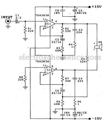
Yesterday I have seen an article about audio power amplifier based on TDA2030AH in a bridged connection with a +/- 15V symmetric PS. According to the datasheet of TDA2030AH displays,TDA2030AH integrates circuits are very cheap and use-full if you want to start a small audio amplifier. The only thing you have to consider is to use a good power supply and heatsink or you’ll risk to burn this precious IC amplifier. The TDA2030 is a monolithic integrated circuit in Pentawatt package, intended for use as a low frequency class AB amplifier. Typically it provides 14W output power (d = 0.5%) at 14V/4W; at ± 14V or 28V, the guaranteed output power is 12W on a 4W load and 8W on a 8W. I have built this circuit and it is totally fine, it works the same way as the monolithic version.About the supply, 15v is not needed to be exactly as it is, it is 12-18v depends on power output desired, and about that split type supply, you can use an ordinary 12v DC supply, just use two polarized capacitors to create a ground line for the circuit.

-
Hello,all I want to ask you some advice or help for my amplifier. I am interested in building a amplifier which is based on two darlington power transistor--TIP142 and TIP147. (This is the datasheet of TIP142 and TIP147: http://www.kynix.com/uploadfiles/pdf65976/TIP147.pdf ) Because It’s the cheapest 150 Watt amplifier circuit I can make. However,I am finding difficulty accepting the differential input should be driven between -45V and +45V. Meanwhile,I think that using PNP transistors for a differential input is quite uncommon today. 1) To meet my criteria I changed parts of the circuit so that the differential input is made of NPN transistors instead that are connected between 0V (common, ground) and the +45V. 2) The output stage has also been modified so that R3 and R5 are on the negative side of the supply (-45V). I moved the driver transistor Q3 to the other side, that is, the +45V making sure to keep the same resistor values. Naturally, Q3 has been replaced by a PNP transistor. 3) In the input stage, differential input, the signal ground has been made the same as that of the differential input stage. I am attempting to build the amplifier with my modifications.Do you have any suggestions to give me? Best wishes~