

exscape
-
Posts
7 -
Joined
-
Last visited
Content Type
Forums
Events
Gallery
Everything posted by exscape
-
R-110SW / R-112SW / R-115SW Repair Blog
exscape replied to ngen33r's topic in Technical/Restorations
The heat isn't very close to the resistor, it's exactly behind the MOSFETs, like literally millimeters from where they are mounted. I have a 5 W for that resistor and moved it to the opposite side of the PCB for now. Though the transistor area gets just as hot as the resistor, both are about 70-73 degrees C. No, they don't matter. I had a look in the datasheet, and as I expected they are date codes and stuff. 9 is the year (2009 according to the datasheet, but perhaps 2019 is also "9"?), 14/20/24 the week, and P means it's lead-free. -
R-110SW / R-112SW / R-115SW Repair Blog
exscape replied to ngen33r's topic in Technical/Restorations
I tried the Klipsch amp with a separate cone (from a guitar amp), at low volume, and indeed the amp works! No tinny sound at all, just bass. It gets DAMN hot though. Towards the top, opposite the knobs (where the MOSFETs are) the plate becomes about 70 C (158 F). That's hot enough that it's painful within 1 second of touching that spot. And this is while delivering less than 1 W into the speaker, volume is enough to clearly hear it across the room but not a ton more. A power meter shows it draws 45 W from the outlet. I'm guessing that much heat isn't normal? Or is it independent of power delivered? -
R-110SW / R-112SW / R-115SW Repair Blog
exscape replied to ngen33r's topic in Technical/Restorations
But since the driver/cone sounds the same on a known-good amp, surely it's broken? It also sounds equally off when you test it with just a 9 V battery. I used the original FET, IRFB4227. I don't think higher-power FETs would fit easily. -
R-110SW / R-112SW / R-115SW Repair Blog
exscape replied to ngen33r's topic in Technical/Restorations
So I finally got the parts, time and energy needed to truly work on the amp, and finished today. I plugged it in and... it makes sound. But not the sounds I want it to make. Listen here: The speaker cone looks entirely new from the front. Could it still be the speaker that's broken, or is the amp more likely? If so, any advice on how to troubleshoot as I have *NO* idea what could cause this? The noise is correlated with the bass in the sound playing. E.g. if you play a kick drum, you get a treble-y noise every time the kick should play. Here is what a 85 Hz sine wave played though the sub looks on the SP+ and SP- terminals on the amp. First, with a large timebase, to show the 85 Hz: Then zoomed way in to show the noise that makes the 85 Hz line so thick: Are these readings as they're expected to be, or broken? Note the weird Vrms readings. The vertical scale is the same, so the noise is clearly far lower amplitude than the signal, yet the RMS voltage reads as about half. Peak-to-peak I'd estimate 20 V vs 4 V based on the vertical divisions alone. Edit: So just after posting I realized I could actually test the speaker alone, by driving it directly from my AVR. Not the best idea, but I figure it's safe as long as you stay at low volumes = low power. Anyway, the speaker sounds like crap this way too, so it's most likely broken. Damn it, all this work and I'm still not done -- and perhaps I can't even find a replacement for a reasonable price. Question 2: How warm is the back of the plate (near the output MOSFETs) supposed to get? Mine gets hot (over 50 C) in just a minute or two of testing, doesn't seem right. Perhaps it's due to the speaker issue? Is it meant to get warm enough that it's hard to touch, especially so quickly? -
R-110SW / R-112SW / R-115SW Repair Blog
exscape replied to ngen33r's topic in Technical/Restorations
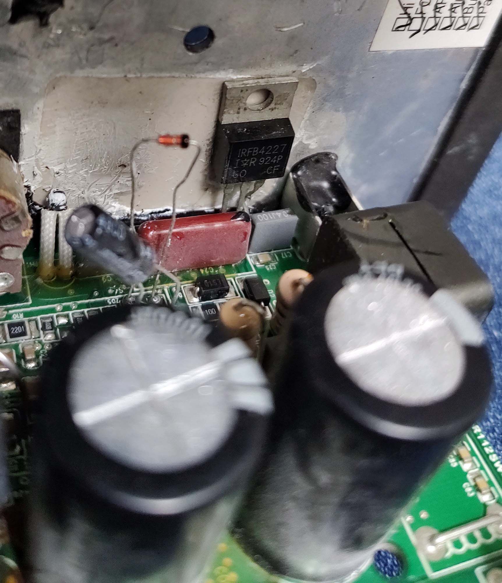
Hello! That resistor is brown-black-black so 10 ohms. Mine measures about 9.8 ohms so that checks out! This is on a R-112SW though but I would assume they're the same. I have a similar question myself. Just above the red film cap in the above photo (next to the electrolytic capacitor) is a zener diode, marked ZD5. Does anyone know the specs for this diode? Mine has been replaced by someone else, with a through-hole diode. I have no idea if it has the correct value or not, so I figure that *if* the amp doesn't work after the changes I have planned, I would have a look at that diode next. My multimeter can't measure the zener voltage, but if someone posts a value I'll build a small circuit to verify it. -
R-110SW / R-112SW / R-115SW Repair Blog
exscape replied to ngen33r's topic in Technical/Restorations
I ordered a couple of IRFB4227 MOSFETs after checking out the reference design (IRAUDAMP7S) and datasheet of the class D amp (IRS2092S) and learning it's designed to use two n-type MOSFETs... ... but I wonder if I have more PCB damage. A few things aren't connected as I expect from the reference design/datasheet. I expect there will be variations, but still. One connection isn't as I expect from the high-side MOSFET (the right one). Could someone check this one on a working amp (or at least one that hasn't had damage to this part of the circuit)? I think there should be a direct connection between source (pin 3) to the VS pin of the driver, which is pin 13, the 4th pin on the right side, counting upwards away from the plate, but I measure 35k and increasing (charging some capacitor). Judging the schematic in the reference design, this pin is used by the gate driver as part of the current loop to the gate pin, so I don't think it can work properly with a 35k+ resistance in there. The equivalent connection for the other MOSFET (VCC- to pin 10, 2nd pin from the bottom on the right side) is 0.07 ohms. EDIT: I typed the wrong MOSFET pin initially (drain instead of source). Fixed now. Another edit: I figured out good connections point to bodge this so it shouldn't be a big issue. I do however believe my driver chip is dead after trying to measure the gate drive signal. I suppose it's possible it doesn't run without the MOSFETs but it shouldn't really know, right? -
R-110SW / R-112SW / R-115SW Repair Blog
exscape replied to ngen33r's topic in Technical/Restorations
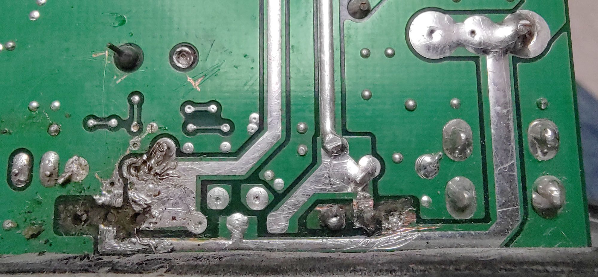
Hello everyone! I just purchased a broken R-112SW, assuming the fault would be the overheated component near that one resistor, but it turns out that while that MAY also be the case, that wasn't the only fault present. Skip until the next heading if you don't want the details of what I've found so far, but rather my questions! Someone else has been in here and replaced stuff prior to me, and apparently they didn't succeed. "That" resistor is a 5 W 820 ohm white one, way up in the air on long legs, so presumably they were aware of the heat issue and tried to work around it. A few others components are also mounted on very long legs though I seriously doubt it helps for those (one of them being a diode, possibly a Zener). Anyway, the bigger problem is that I only have one output transistor, and I assume two are supposed to be there. I haven't found ANY pictures of them though, so I'd be very thankful if someone with a R-11x amp could check theirs! The one that IS there doesn't have the white weave(?) present on other images I've seen (all with the transistor "cover" on, hiding the information I seek). The back of the board is also damaged around the transistors, either when they blew or when someone tried to repair it. There's a short between the + and - rails on the amp board (the PSU works, unless connected to the amp). I haven't diagnosed this one yet; there are some suspect traces that seem to run very close to one MOSFET pin where there's some PCB damage, but it could also be e.g. the cap across the rails. EDIT: I solved this one, the short is visible in my picture (PCB back), bottom left, some kind of copper wire strands (or solder wick strands) were shorting them. There's still a short between one supply rail and the output though. The 22 uH inductor on the output also appears blown, there's a crack in the casing. I can only check the DC resistance though and it reads as 0.05 ohms (after nulling out the probe resistance), and I have no idea what to expect for an inductor in powerful class D amp. EDIT: I just noticed this crack exists on your pictures too, and a DC resistance of 30-50 mOhm is pretty expected, so there's not really any evidence it's blown. My questions a bit more succinctly: 1) Could someone post pictures of the output MOSFETs (and the component(s) in between them if any) and their exact part numbers? I have a badly soldered IRFB4227 there on the right, and nothing but a scarred PCB on the left. I've no idea if the other is supposed to be P-type or N-type as this is my first class D amp; I've found designs with 2x N-type and designs with complementary pairs. I don't even know if the 4227 is correct since it's clearly been tampered with. 2) Pictures of the back of the PCB around the MOSFETs would also be truly excellent. I don't know exactly where the left MOSFET is supposed to be connected, nor do I know what part of that mess (see my photos!) is correct and what isn't. 3) Any ideas on what kind of ripple is OK on the PSU? I haven't checked with my scope yet, but my multimeter suggests 4 V AC is present on the 57-ish volt rails! And the frequency reads as about 400 Hz? I don't trust that fully though and will check more carefully unless this is to be expected. Edit: I checked on the scope and there's no worries. The noise is about 170 mV peak to peak at ~550 kHz. 4) Any other general advice? Thanks in advance